JRP Innovations

JRPi Tech Blog

Write-ups on my experiments and experiences in everything from embedded C++ to Windows software support. Additional information about freelance services are also provided.
  • Posted on

    I Tried to Dump the Firmware From a UE Wonderboom. I Found 2.4 Seconds of Sound Effects Instead.

    The story of reverse-engineering a first-generation Bluetooth speaker, one mystery test pad, improvised SPI programmer, and 1 tiny puff of magical electric smoke at a time.

    Project: Ultimate Ears Wonderboom (Gen 1)
    Main SoC: Airoha AB1520
    External flash: Fudan FM25Q08A, 8 Mbit / 1 MiB SPI NOR
    Research: October 2026
    Status: External flash dumped and decoded; main firmware still evades extraction so far


    Now, many people may wonder why bother.

    In today's era most of our decade old accessory devices are "Good enough" for normal use still. Though my good enough is different than other peoples; if I know a device is technically capable but it has behaviors that bother me, or needs a custom feature. I have gotten accustomed to taking it apart and hacking it.

    The goal here was, (and still is), to access the device firmware and modify the auto-off interval. The default behavior for the Gen1 Wonderboom is to automatically turn off after 10 minutes without an active audio stream. For a Bluetooth speaker that lives on my desk and gets used for work, this is annoying to say the least.
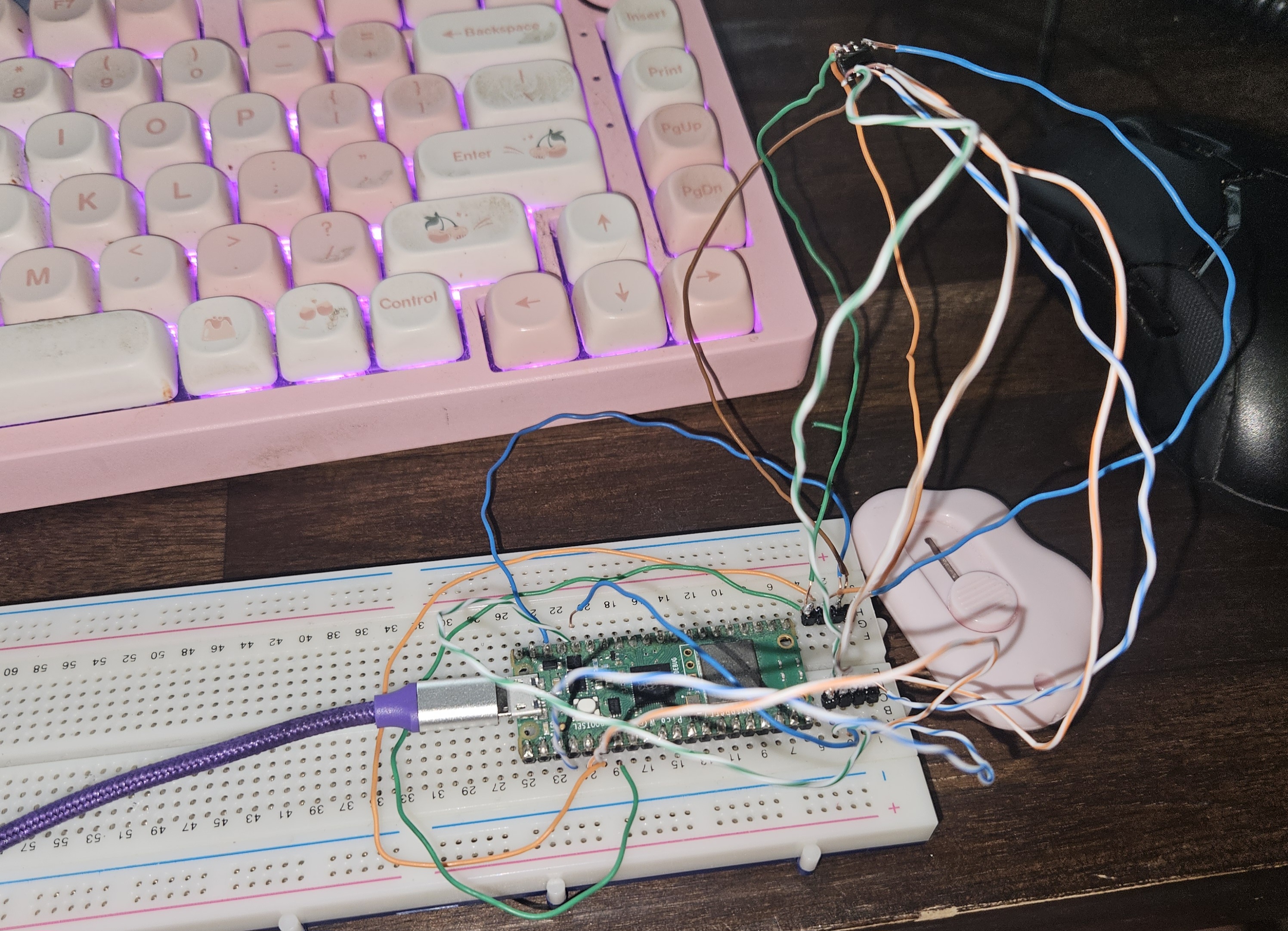
    The questionable final result of DIY and a refusal to buy tools...

    There is a special kind of optimism involved in spotting an eight-pin flash chip on a Bluetooth speaker's motherboard and thinking, "Gee, this is going to be easy. I'll just dump the firmware."

    That is how I ended up taking apart a first-generation Ultimate Ears Wonderboom, trying to get low level access to an Airoha Bluetooth SoC, making power components release their magic smoke, hand-desoldering a tiny SPI flash chip, and wiring it to a Raspberry Pi Pico with solid-core copper wire.

    The punchline? I successfully recovered the chip's entire contents. It wasn't the firmware. It was, for the most part, two little audio cues. Just the start-up and shutdown sounds. Even funnier, the device runs stable with the flash removed entirely.

    That sounds disappointing, and for the specific goal of extracting the main firmware, it absolutely was. But as a reverse-engineering project, it turned into a surprisingly useful map of how this speaker is put together—and a lesson in why a successful memory dump and a successful firmware dump are not the same thing.


    The target: an original Gen 1 Wonderboom with an Airoha AB1520
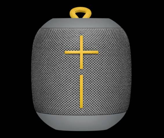
    Wonderboom 1 stock image

    The original Wonderboom is a fairly ordinary-looking portable Bluetooth speaker, if you're under 50 we've all seen one at this point. Under the shell, though, it's a collection of distinct subsystems: battery management, amplification, speaker drivers, physical controls, and the Bluetooth/audio controller.

    I did a complete teardown as shown here on YouTube by Mike Novelli. The main deviation being that once I seperated the top PCBs (The main motherboard and the audio driver daughterboard), I didn't continue to disassembling the lower battery assembly.

    As I examined the boards and began reverse engineering I identified the Airoha AB1520 alongside a Fudan FM25Q08A serial flash, as well as Texas Instruments components for charging, power conversion, and amplification. My target is the Airoha AB1520, handling the Bluetooth side of the operation.

    That external flash looked like the obvious starting point. An 8-Mbit SPI NOR chip seemed large enough to hold a modest embedded firmware image, and it's a familiar target for hardware reverse engineering.

    But before I got to it, I had to probe through the first temptation, the low hanging fruit: the row of labeled factory test points. You can see them on the top board on the image above (The gold tinned holes near the buttons), the flash chip is directly adjacent and the Airoha chip label next to it is visible on the mainboard as well.

    If you zoom in close enough, you may see yourself that they were nice enough to leave them labelled!
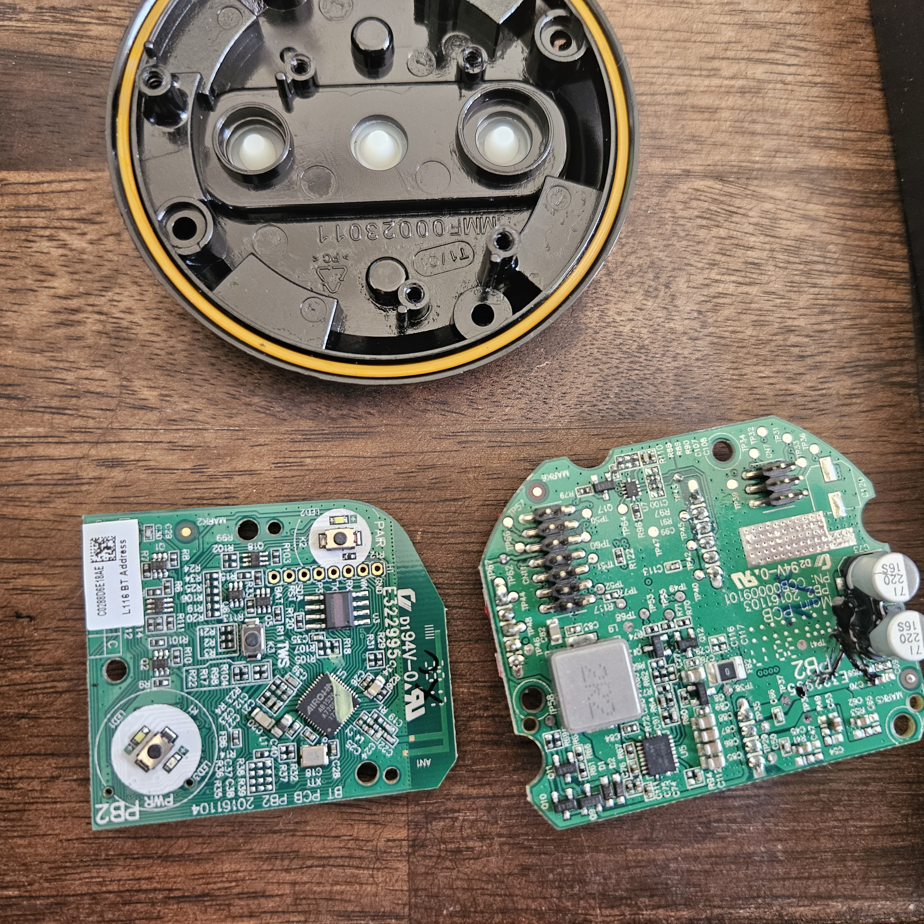
    The AB1520 Bluetooth board, before I started negotiating with its test pads


    The red herring of test-pads on locked down devices...

    This is the information they were nice enough to grace us all with:

    GND   WK   RX   TX   P3   SDA   RST   BAT
    

    The wheels were turning in my head and the layout looks an awful lot like something a factory programming or diagnostic fixture might use: power, ground, wake, reset, UART, and two other control signals. Simple enough! (I thought!)

    At this point I soldered on headers, connected my USB serial adapter and went to town. Er, tried to go to town, if I'm going to continue this allegory, all I did was put on my coat and touch the door handle. More on the UART and serial findings in a minute.

    As soon as I realized I needed more information than aimlessly probing for UART; the first thing I did was measure voltages with the battery installed and the speaker in different power states. With USB disconnected and the serial adapter removed, the results were:

    Test pad Speaker OFF Speaker ON
    WK ~0.1–0.2 V ~4.21 V
    RX 1.800 V 3.25 V
    TX 1.800 V 3.25 V
    P3 1.469 V ~3.00 V
    SDA 1.470 V ~3.00 V
    RST 0 V 0 V
    BAT ~4.26 V ~4.25 V

    The interesting part was the pairing. RX and TX moved together between 1.8 V in standby and 3.25 V while running. P3 and SDA also moved together, though at slightly lower voltages. That suggested power-state-dependent I/O biasing or supply behavior, but it did not prove which regulator powered each pad or that the SoC was switching its entire I/O domain.

    WK was odder still. I accidentally touched it to ground while probing and the speaker woke up. That's a useful clue about the wake circuitry, though not enough to establish the exact active polarity of the AB1520 input.

    I also found documentation for a different AB1520-based module, LG Innotek's WB1NB7, which describes PIO3 as MODE_SEL (test mode selection) and SDA as CALIBRATION (engineering test mode). That was encouraging—but it's a reference design from another product, not a Wonderboom programming manual, and at best just acknowledgement the CPU could be configured this way.

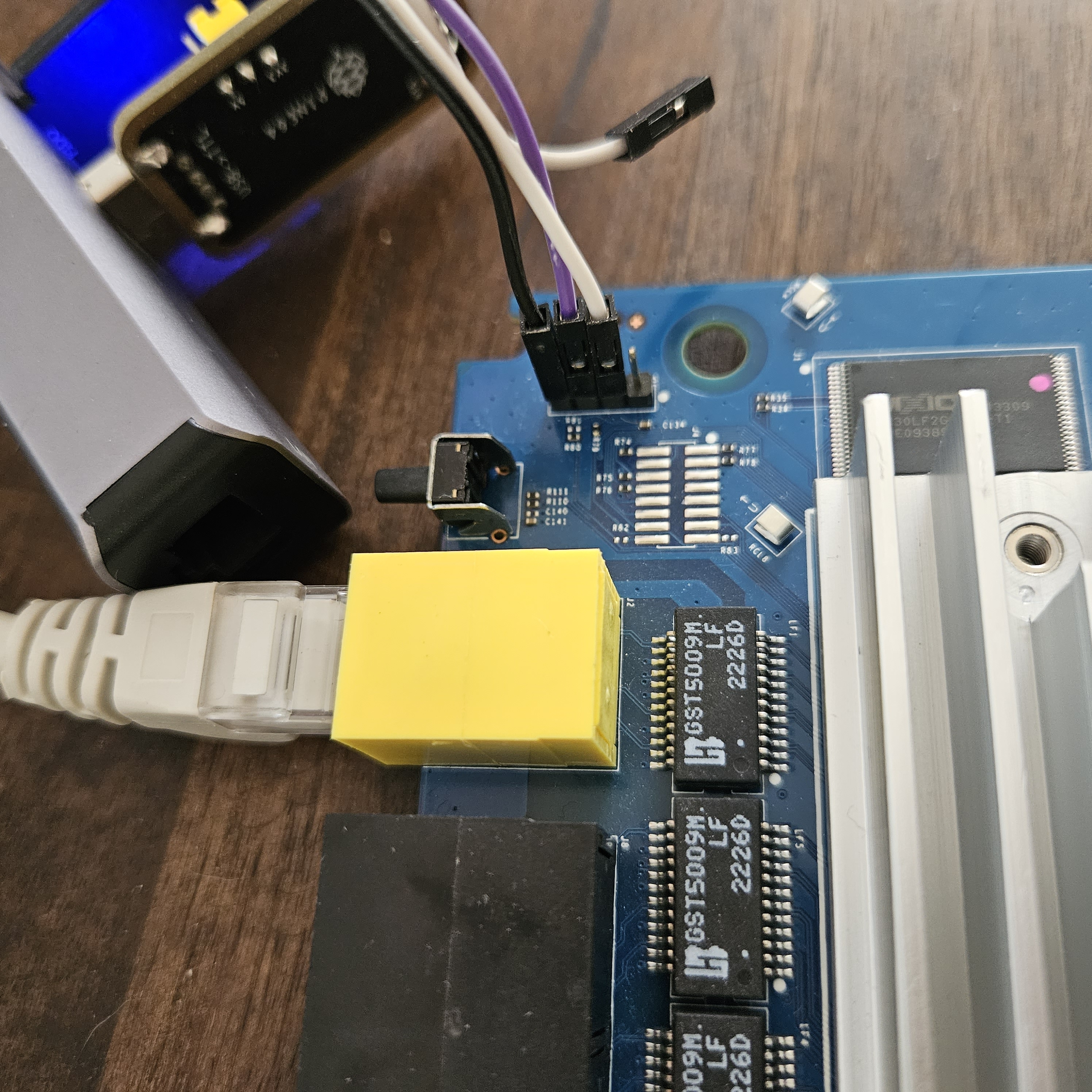
    In the image below, you can see my "beautiful" hand soldering job of adding headers to the pins on the main board.
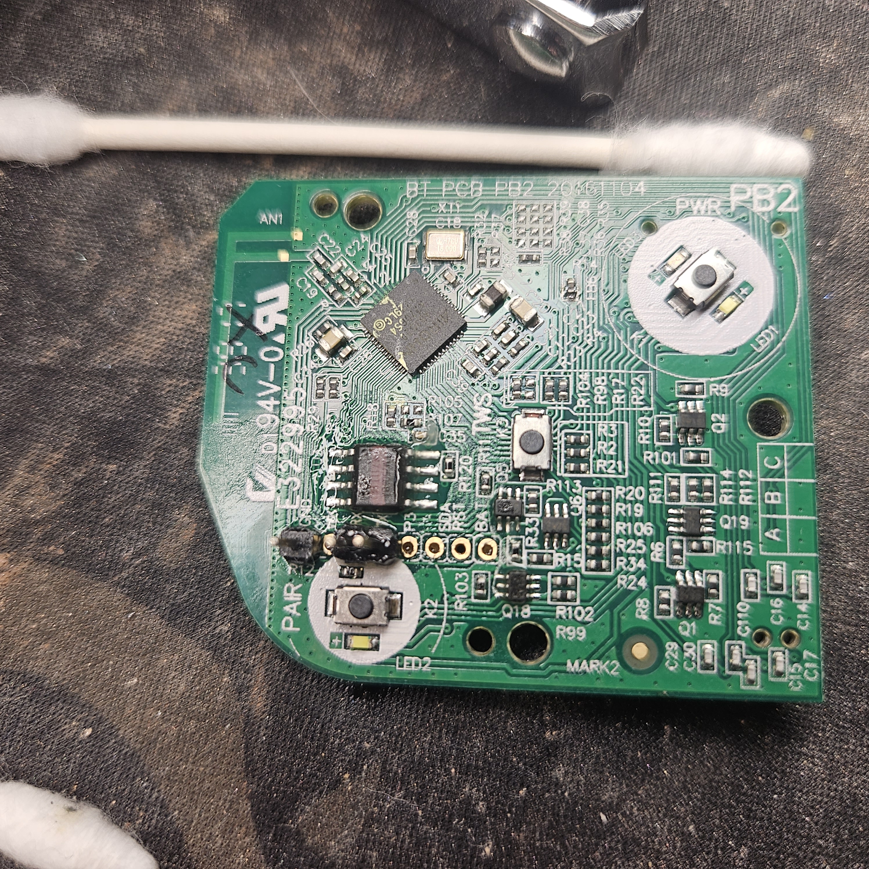
    The massacre begins


    UART: a handful of bytes and absolutely no conversation

    Naturally, I went after RX and TX first. I connected my USB serial adapter and captured raw bytes at 115200 baud during power-on.

    What came back was not exactly a warm welcome:

    39 ff
    2d fe
    14
    

    After swapping which board pad fed the adapter's receive input, I got more tiny, inconsistent bursts:

    9c fe
    08 fe
    90 fe
    3d
    

    I eventually did a useful isolation test: with only the adapter's ground connected, I received no spurious bytes. With the receive input attached to either the board's TX or RX pad, boot-time junk output returned.

    This was likely just evidence of electrical transitions and level shifts on the nets like I was discussing in the previous section registering weird as the device went from 1.8v to 3.3v. Ultimately I got no evidence of a working 115200-baud console.

    I considered turning a Raspberry Pi Pico into a logic analyzer. I still think that's a sensible next step. I also had absolutely no desire to set up an oscilloscope just to stare at two disappointing pins, so the UART investigation stalled here for now.


    Factory mode, I²C deadlock, or just an expensive way to freeze a speaker?

    Next came P3 and SDA.

    Briefly grounding P3 during normal operation and during a power-on attempt did not expose a useful mode or diagnostic interface.

    During one P3-related experiment, I tried shorting it while the device was already powered on, that's when I got the fresh smell of the earlier mentioned magic smoke. I couldn't identify what I fried, couldn't find an obviously burned trace, and didn't observe abnormal heating afterward. The Wonderboom continues to operate completely normal as far as I can tell, which is encouraging! I surely fried something there but this stunningly locked down device at least has well designed power rails!

    SDA was much more interesting to play with.

    When I held SDA LOW during startup, the speaker entered a repeatable, abnormal state: the usual power indicator and the red low-battery-style LED remained solid, and the power button stopped responding. Both UART pads still sat high, but still, nothing useful appeared over serial.

    There was one key observation: releasing SDA didn't unfreeze it. I had to remove power from the board and restore it before normal behavior returned.

    I had found a reproducible startup failure or alternate startup path. What I hadn't found was proof of engineering mode. On the related AB1520 module docs I found, SDA is explicitly associated with engineering calibration, but SDA seems to be a conventional I²C data signal. Holding it low at startup could might block firmware read transactions and leave the CPU hanging indefinitely.

    Without an SCL capture, a documented mode-entry sequence, or a response from a known protocol, the honest label I gave this experiment is “Hung SDA-dependent startup state, cause unresolved.”

    I also located three pads on the underside marked A, B, and C. At least two traces appeared to route toward the main SoC. Their purpose remains unidentified. I have yet to probe them at all due to their inconvenient location.

    They may be JTAG or SWD, maybe not, but it's one of my next things to look at because they're mysterious and near the processor.
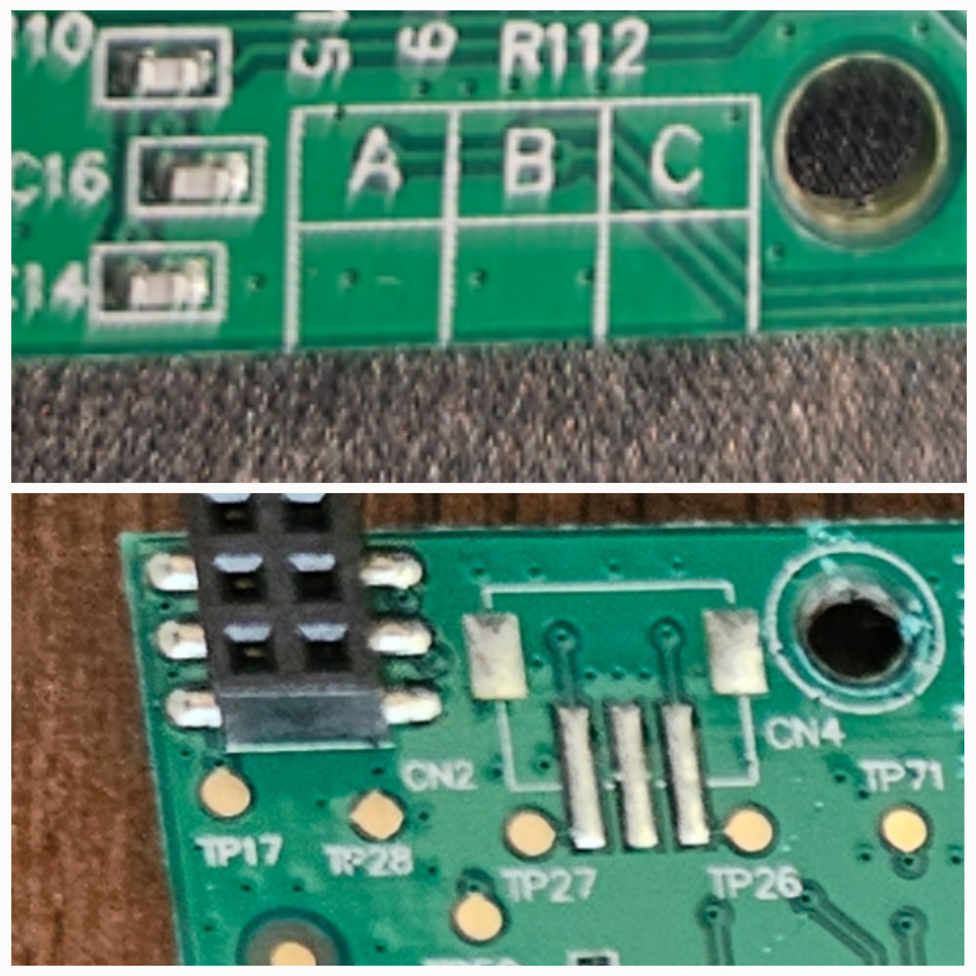
    UNDERSIDE A/B/C


    Fine then. I'll just dump the eight-pin flash chip.

    By this point I was tired of trying to coax the AB1520 into a conversation. The external flash was right there, and I can hack together a way to read and ordinary SPI NOR with my existing equipment.

    There was only one problem: I didn't have a dedicated programmer or a comfortable chip-removal setup, like a reflow station, handy. (Don't worry, I've ordered them.)

    So I improvised! I hadn't done this in a while so I practiced hand-desoldering a similar flash another IC and discovered I was entirely capable of damaging it. Then I decided to remove the Wonderboom flash anyway, because f*** it we ball.

    I added Sn63Pb37 solder to the existing joints and bridged them to add mass and lower the leadless factory solder's melting point with plenty of flux and a broad soldering-iron tip, eventually I got the chip off with no damage.

    A hot-air station would have been sane and taken way less time, but sometimes it's better to hone your old skills and pretend it's 1992. The old-fashioned approach worked this time.

    Once the chip was free, I soldered solid-core copper leads to it from a stripped ethernet cable, connected it all to a breadboard, then connected that to a Raspberry Pi Pico, and loaded pico-serprog so that flashrom could use the Pico as a programmer. That brings you up to speed on how I got to the picture at the start of this post.

    The flash was now off-board, I gave it the freedom most Chinese chips yearn for and can only dream of. I did this so I wouldn't need to worry about the AB1520 contending for the SPI bus or accidentally back-powering the entire thing through a Raspberry Pi Pico at 3.3v.

    With no socket, no dedicated flash programmer, and considerably more optimism than was warranted I pressed forward.
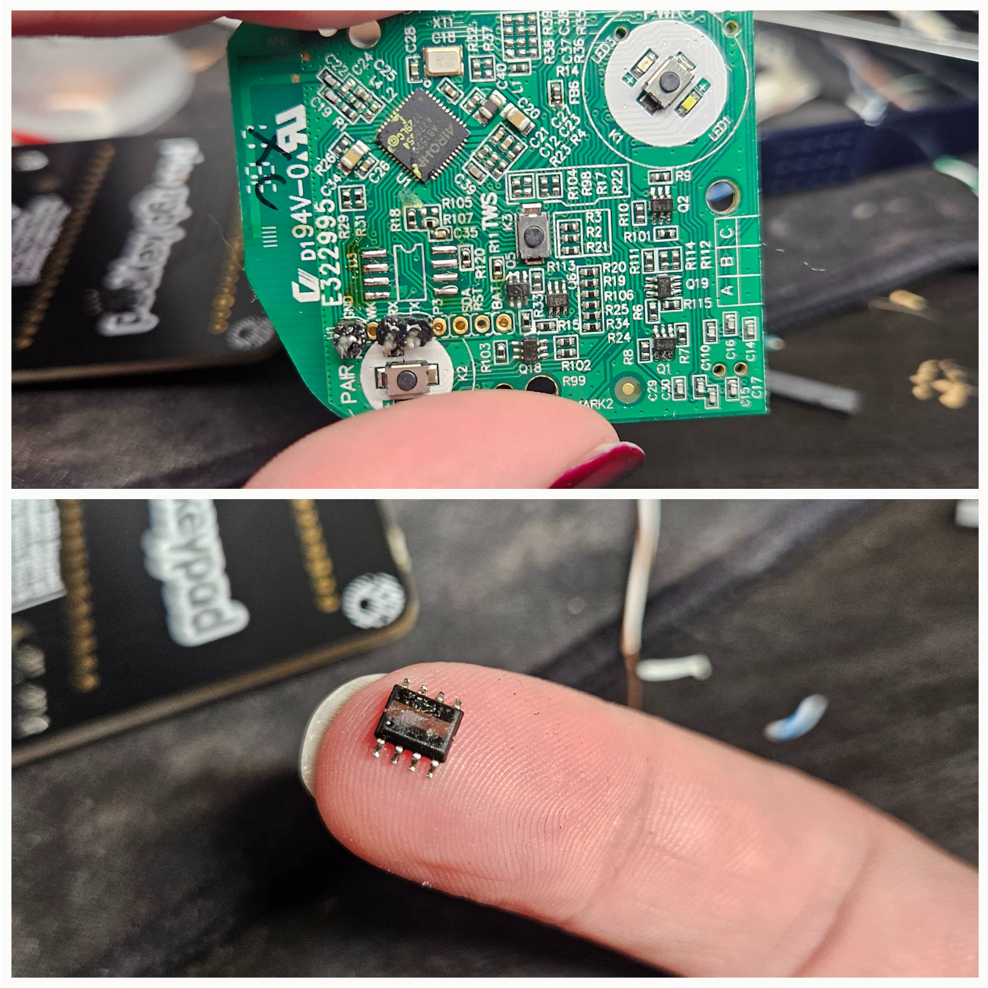
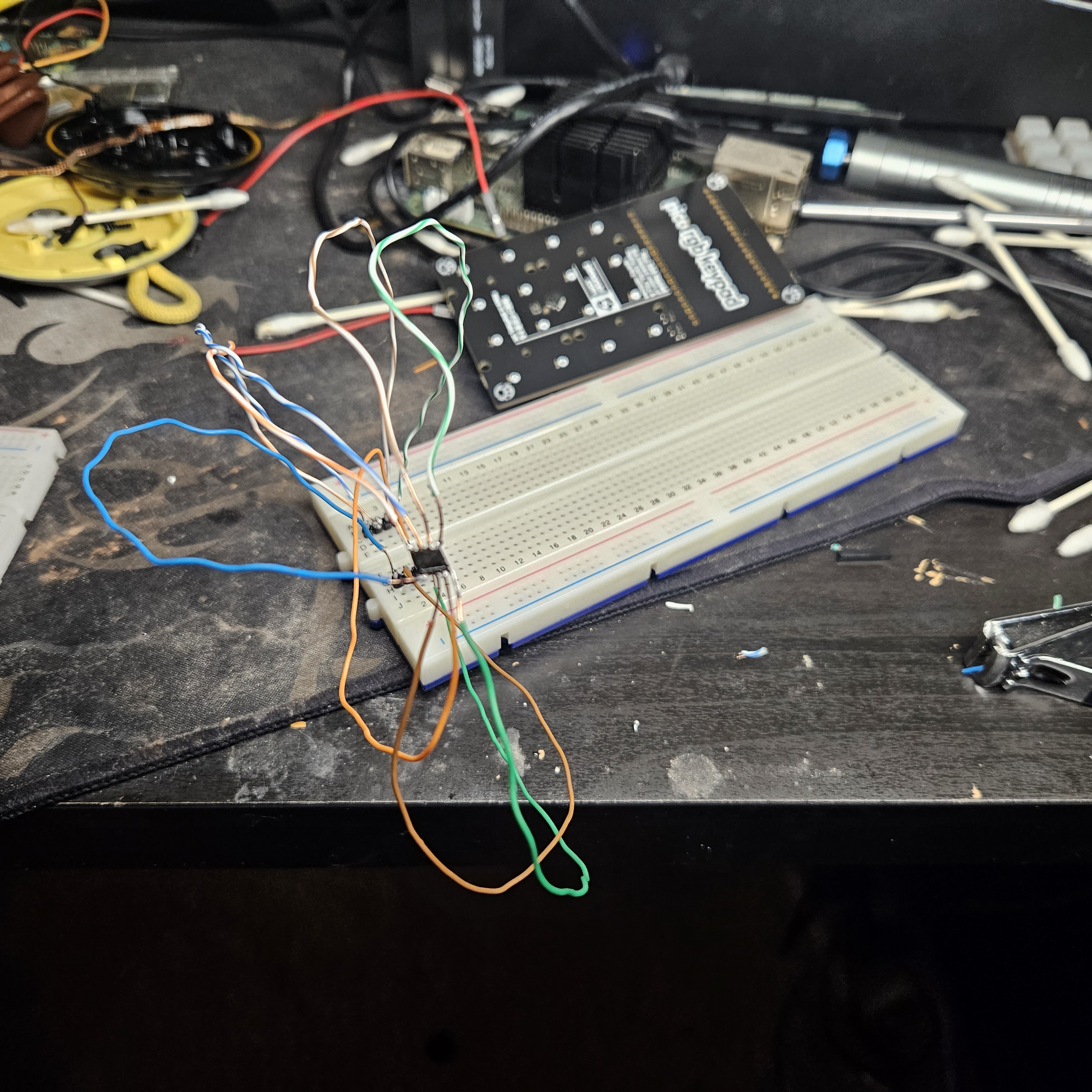
    The liberation of Chinese media The hand-soldered monstrosity


    The flash pin that almost made me rage quit: HOLD

    My first attempt to identify the chip failed:

    serprog: Programmer name is "pico-serprog"
    Warning: NAK to query operation buffer size
    No EEPROM/flash device found.
    

    The Pico was communicating with flashrom, but flashrom couldn't see the memory device. I measured all eight flash pins at rest and found the critical detail:

    Pin:  1    2    3    4    5    6    7    8
    Volts 3.3  0    0    0    0    0    0   3.3
    

    Pin 8 had 3.3 V, pin 4 was ground, and chip select was high. But pin 7, HOLD#, was at 0 V. After reviewing docs I found on this SPI flash, asserting HOLD# can suspend ordinary serial communication. Pin 3, WP#, was also low; but write protect being enabled is fine for now and shouldn't disable any reads.

    After bringing HOLD# HIGH, leaving WP# as it was, flashrom reported:

    Found Fudan flash chip "FM25Q08" (1024 kB, SPI) on serprog.
    

    WOOHOOOOO! That was my breakthrough. The chip survived removal and was actually responding.

    One caveat for anyone copying this: the flash's WP# and HOLD# pins can serve as Quad-SPI data pins in other modes. I used a direct HIGH connection in the successful identification experiment, but proper resistor pull-ups would be best practice.


    Two clean reads. Both perfectly matched by hash.

    The successful read command was:

    .\flashrom -p serprog:dev=COM13:115200,spispeed=1M -c FM25Q08 -r wonderboom_original_1.bin
    

    I read the chip a second time into another file and compared hashes:

    wonderboom_original_1.bin   1,048,576 bytes
    wonderboom_original_2.bin   1,048,576 bytes
    
    SHA-256 (both):
    A1F09CBA925F1BB239001D87D3FD80796E959B8BC095E89D2A810C5084A136DD
    

    Two complete 1 MiB images. Identical SHA-256. I also kept the original flash untouched. The experiment had finally produced something meaningful and reproducible.

    Then I opened the binary.


    The twist: 95% zeros, 900 SBC frames, and two sound effects

    The first surprise was that the dump was 94.9% zero bytes. Most of the nonzero data lived near the beginning of the address space. The next surprise was that the interesting region had a coherent resource layout, not the shape of any conventional executable image.

    The inferred top-level directory described four resources:

    Offset Length What it appears to contain
    0x001000 1 byte Placeholder/unknown
    0x002000 57,600 bytes SBC audio stream
    0x011000 25 bytes Index describing two clips
    0x012000 0 bytes Empty resource

    At 0x002000, frames began with 9C F5 0D. 0x9C is the synchronization byte for SBC, the Subband Codec widely associated with Bluetooth audio. The 57,600-byte payload held 900 consecutive frames, each 64 bytes long, consistent with 48 kHz, dual-channel SBC audio.

    The 25-byte index split those frames into two clips:

    Clip Frames Duration
    1 432 1.152 seconds
    2 468 1.248 seconds
    Total 900 2.400 seconds

    I decoded both streams with FFmpeg. They were real, non-silent audio—not random bytes that happened to resemble an SBC header. Obviously the resource format and index layout are only inferred from this dump, not an official Airoha specification, but the offsets and lengths reconcile exactly, and the rest is just 0's.

    At this point I had to ask the obvious question: If I removed the external flash, would the speaker even boot?

    This whole thing was starting to feel like a sick joke after spending several hours of my life in a labor of love, just so I wouldn't have to buy a new speaker.


    I powered it on without the flash. It worked.

    It powered up. It still worked as a Bluetooth speaker. But its familiar power-on and power-off sounds were missing. The Bluetooth connection/join sound still played.

    The conclusion is narrow but strong: the external FM25Q08A is not required to boot the Wonderboom's normal application, and it seems like only two user-interface sounds live on it in the first place.

    The natural next hypothesis is that the real Bluetooth/application firmware lives in storage associated with the AB1520, perhaps embedded flash. But I have not dumped the SoC's program storage, yet. This seems like it should be do-able over Bluetooth but sometimes you have to put a project down for a few weeks until you can stomach looking at it again after surmounting the dissapointment.

    So yes: I went looking for firmware, and the tantalizing 1 MiB flash chip turned out to be, apparently, an audio-resource cartridge. Maybe not a deliberate red herring from Ultimate Ears, but it was a very effective one from my perspective.


    What I actually learned—and what's next

    Despite the detour, this project produced results I can repeat and build on:

    • Identified the AB1520 controller and external FM25Q08A on the original Wonderboom board.
    • Documented the main factory-pad labels and power-state-dependent voltages.
    • Confirmed that 115200-baud UART probing has not yet yielded a verified debug interface.
    • Found a reproducible SDA-dependent startup lockup, although its cause remains unknown.
    • Located three more uncharacterized underside pads marked A/B/C.
    • Removed the flash, identified it using a Pico and flashrom, and recovered two identical 1 MiB dumps.
    • Reverse-engineered enough of the resource container to extract and decode two SBC sound assets.
    • Verified through a flashless boot test that the external memory is not required for normal application startup.

    There are two paths forward. The practical one is a custom sound-resource pack: encode replacement clips with compatible SBC parameters, preserve the directory structure, and test them on a replacement flash while keeping the original image safe. That's a tangible modification already grounded in a format I can parse.

    The harder—and still more interesting—one is accessing the AB1520's actual firmware. That means identifying what A/B/C do, finding the real reset and engineering interfaces, and locating an AB1520-specific bootloader, factory tool, or readback path. The related LG module documentation is a lead, not an unlock procedure. An oscilloscope or logic analyzer would probably help, whether I feel like setting one up or not.

    For now, I have not recovered main firmware, no custom firmware execution, and no confirmed factory debug console. Those are the next research goals, sadly not accomplishments I can claim today.


    Final thoughts

    I started this thinking I'd find a firmware image in a convenient external flash chip. Instead, I learned how the Wonderboom handles at least some of its audio assets, recovered an undocumented little resource container, and proved that its main application can run without that memory installed.

    And the Raspberry Pi Pico earned a permanent place in my reverse-engineering toolkit. A board that costs less than a decent lunch, a few lengths of copper wire, and open-source tools are enough to extract a bit-perfect image from a chips removed by hand. That's a learning lesson for everyone with the know-how.

    The main firmware is still hiding. The underside test pads are still suspicious. I still don't know which component sacrificed itself to make that puff of smoke.

    But now we know exactly where ~2.4 seconds of the Wonderboom's personality were hiding!

    To be continued.


    References and tools

    Research note: Experiments were performed on one board. The original binary dump is preserved with the SHA-256 shown above. Potentially damaging tests, especially those involving an unknown pad or a lithium-ion-powered circuit, should not be treated as a general-purpose procedure.

    If you have any additional information to aid my efforts or would like the recovered flash blobs, reach out to [email protected]
  • Posted on

    Reverse engineering is something I have been learning for years, most reverse engineering projects when you're learning end in confusion, destroyed devices, and breaking things to figure them out...

    I wish I started my journey with this project! By the end of the first day, I had a root shell, a full extracted firmware filesystem, the stock update image unpacked, the bootloader command list, the actual compressed kernel, several device trees, and a much better sense of what not to type into CFE, (CFE is Broadcom's network device firmware and bootloader for ARM SBCs).

    The short version is: this router is a surprisingly capable ARM Linux system wrapped in several layers of Broadcom and Netgear boot infrastructure. Though, there is also no security??

    Model caveat: My stock update image is for an RAX10 running firmware V1.0.20.174, but an early CFE boot capture identifies its board ID as RAX60 and looks for RAX60.dtb before falling back to a generic DTB. I have not yet reconciled that mismatch. For now, the claims below are about this captured BCM6755 firmware/platform combination, not necessarily every retail unit with either model number. It seems like the firmware between all RAX models may be the same with actual model-specific data passed in from CFE but that's a lofty claim to make and I'm only making it based on this weird identifier mis-match and the DTB handling behavior we will discuss later.

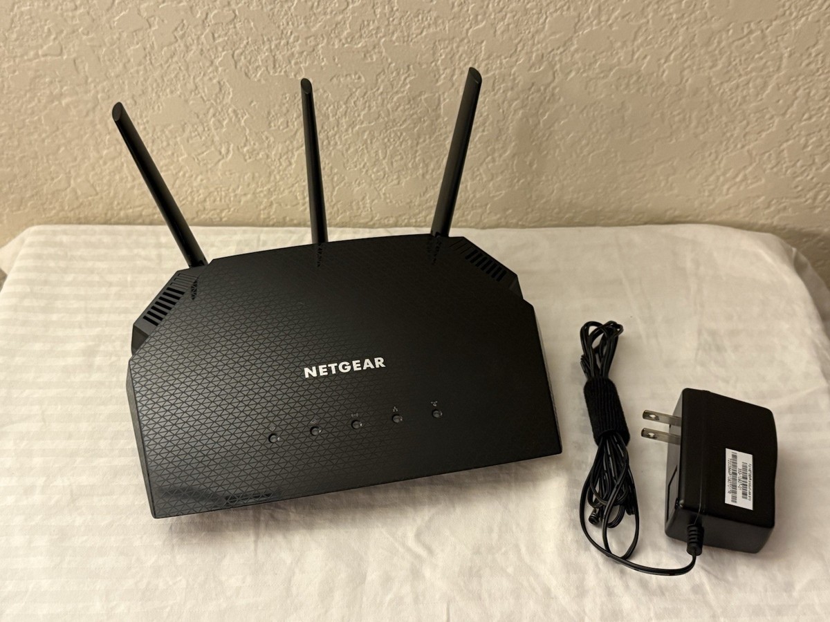
    Netgear RAX10 base

    Dissasembly

    I started with the obvious steps of taking it apart, there were 3 security screw holding the case together, there is a through-hole design mounting the PCB securely into the case. Once the 3 exterior screws were removed and the case cracked, I immediately noted a 4 pin header and had a suspect for serial connection. There was 3 other hardware points with potential for debug/extensibility, though no more on that for now.

    The DRAM (DDR3), the main SBC CPU package, the ethernet controller were all located under a large heatsink. The heatsink was easy to remove with 4 chunky Phillips head screws holding it down exposing EMI shielding with thermal pads for the CPU & Ethernet Controller. Fortunately the EMI shielding was pressure fit and easy to remove without severely damaging. There was an additional chip with it's own EMI shielding directly adjacent the main SBC package, (I suspect this to be radio related though I did not note down the IC label as I already identified my main points of interest for now, this will probably come back to bite me).

    Hardware packages:

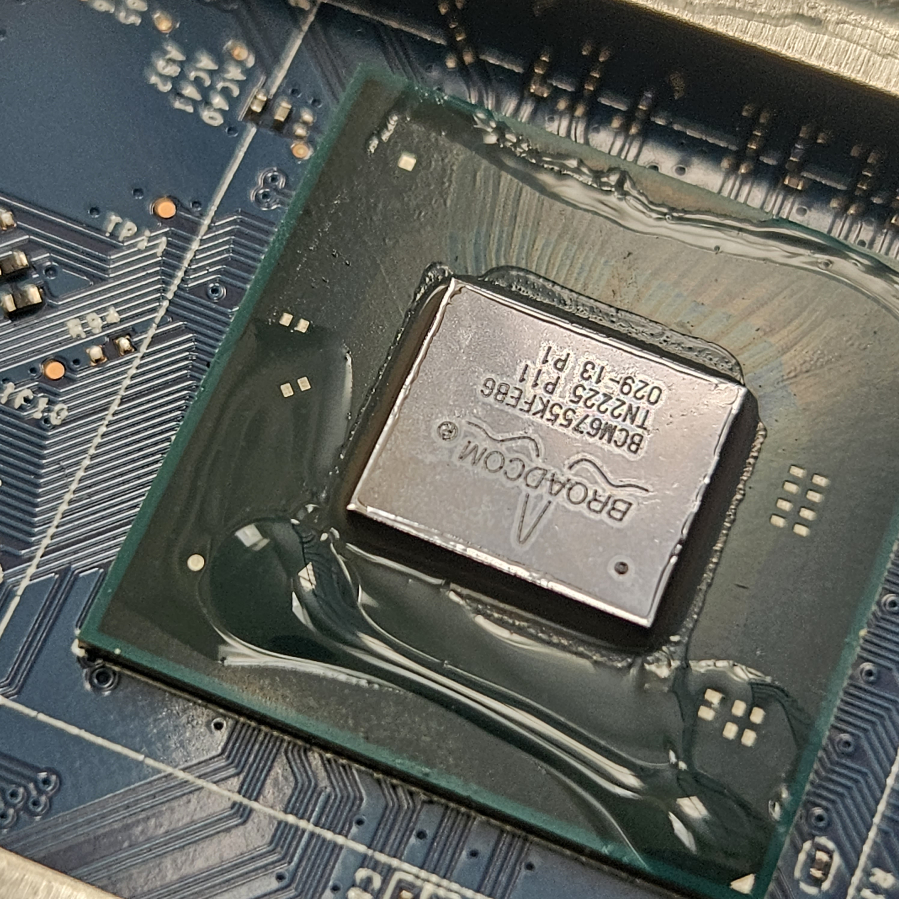
    • Broadcom BCM6755A1KFEBG, SoC
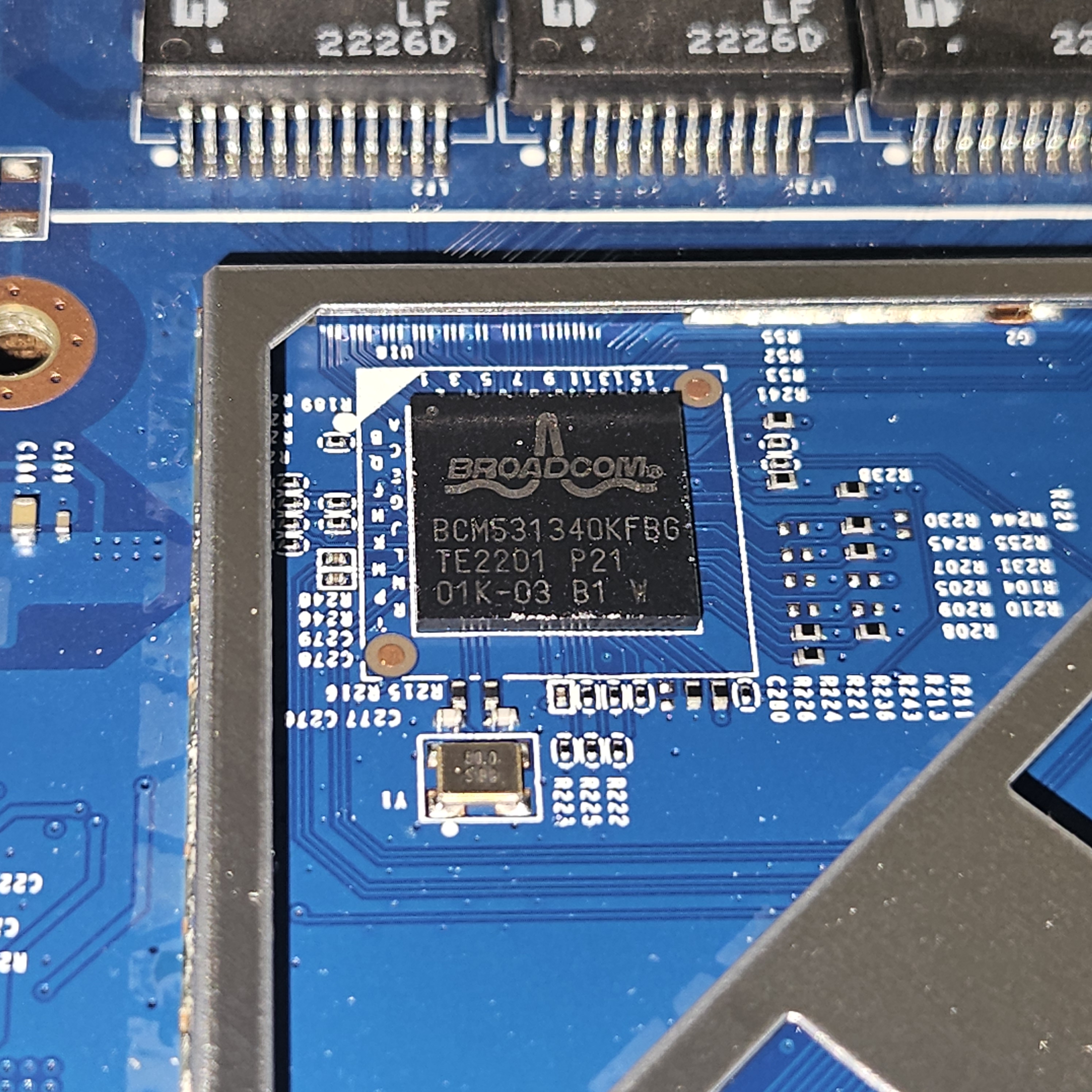
    • Broadcom BCM531340KFBG, Ethernet Controller
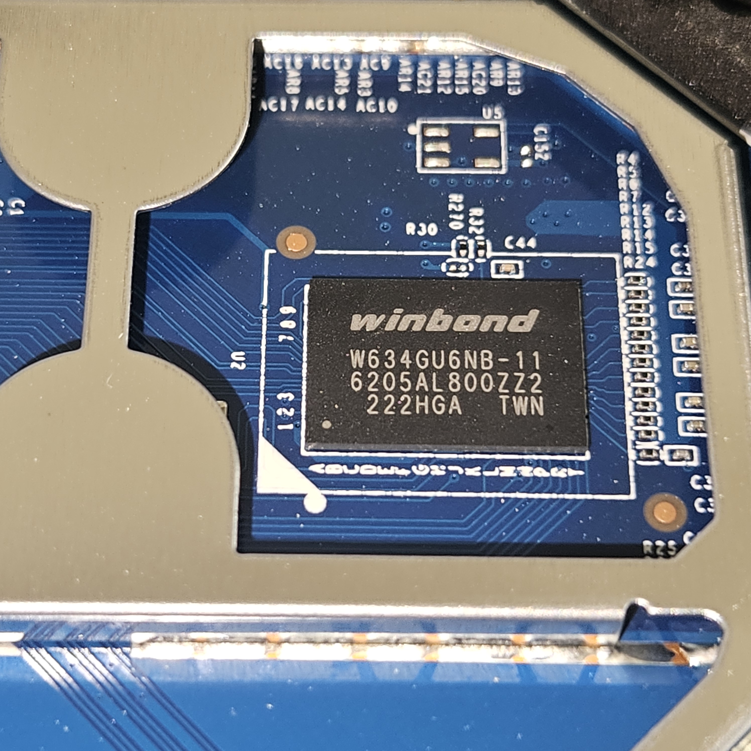
    • Winbond W634GU6NB-12, 4Gbit(512MB) DDR3L RAM RAX10_Main_CPU_BCM6755RAX10_EthController_BCM531340RAX10_DRAM_W634GU6NB

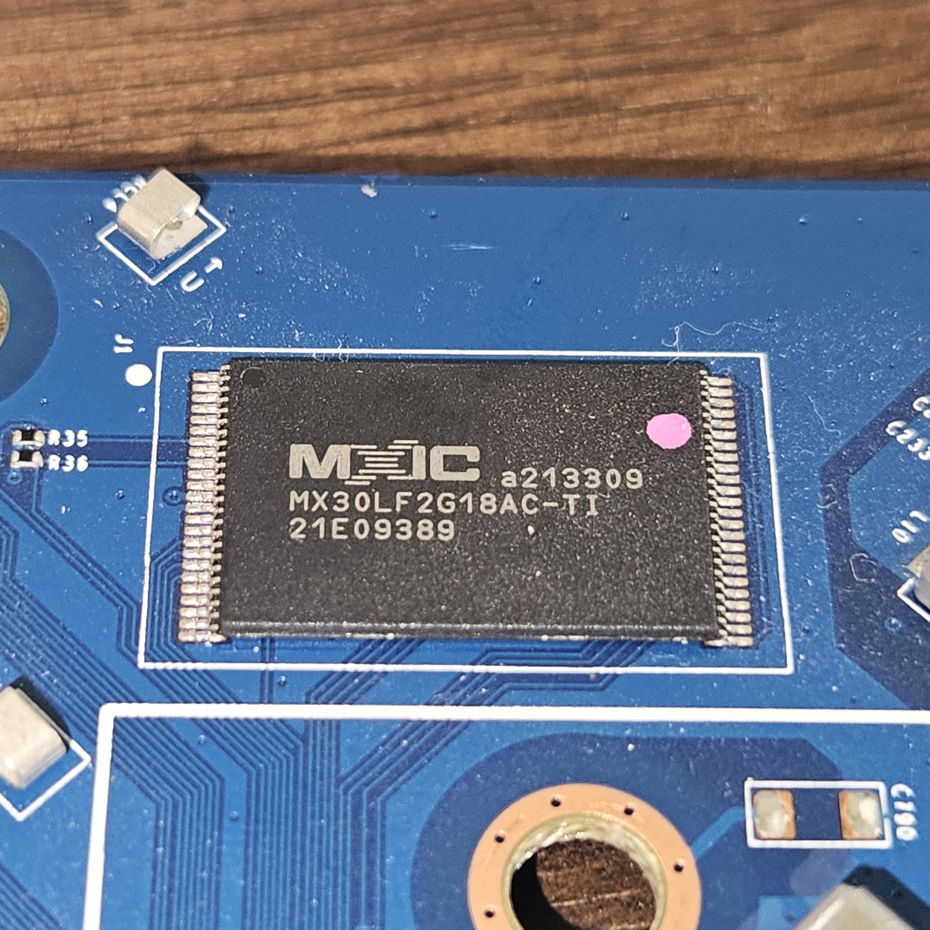
    Seperate from the heatshield, we had the 256MB flash. * Macronix 2Gbit(256MB) NAND MX30LF2G18AC RAX10_NAND_FLASH_MX30LF2G18AC

    That means this is not a toy microcontroller router. It is a 1.5 GHz quad-core ARMv7 Linux machine with half a gigabyte of RAM, hardware packet acceleration, two PCIe Wi-Fi radios, and a slightly cursed 256 MB NAND-backed appliance filesystem; (The NAND is being managed/controlled by the host directly).

    At this point I was ready to see if what I suspected to be a serial header, really was simply a serial header. I got my multimeter and identified voltage as 3.3v, I checked to see if there was any visible voltage change from transmission drops on any of the pins, quickly I identified pin 1 for TX this way (white), I connected it to a standard serial reader after confirming pin out as p0(3.3v) P1(TX) P2(RX) P3(GND), I connected TX, RX, & GND to my Pine64 serial console. RAX10_SerialPort_UART

    I rebooted and opened a standard serial terminal over the USB COM port @ 115200 Baud (115200 8N1), this caused a flood of coherent serial output leading me to re-assemble the EMI shielding and heatsink before the device got too hot.

    The running hardware

    The bootloader identified the platform as:

    Chip ID: BCM6755_A1
    ARM Cortex A7 Quad Core: 1500MHz
    Total Memory: 536870912 bytes (512MB)
    NAND flash: 256MB
    

    The flash is SLC NAND with:

    Page size:        2048 bytes
    OOB/spare area:     64 bytes
    Erase block:    131072 bytes / 128 KiB
    ECC:            BCH-4
    

    The boot chain

    The serial console exposed the full chain:

    Early bootstrap / BTRM
    → Broadcom CFE bootloader
    → CFE reads NAND and locates vmlinux.lz
    → CFE decompresses the Linux kernel
    → CFE loads a DTB
    → CFE patches boot arguments and NVRAM into the DTB
    → Linux boots
    → Linux mounts the SquashFS root filesystem
    

    Identifying CFE lines were:

    ubi_find_file: got vmlinux.lz  size 2756881
    Decompression LZMA Image OK!
    Entry at 0x00018000
    
    cfe_fs_fetch_file: file RAX60.dtb not found
    ubi_find_file: got 947622.dtb  size 4540
    
    Setting ROOTFS: root=/dev/ubiblock0_0 ubi.mtd=0 ubi.block=0,0 rootfstype=squashfs
    CFE appending "isolcpus=3" from PROFILE to boot cmdline
    Appending CFE version to dtb
    Appending NVRAM to dtb
    

    This immediately explained something that confused me at first: the kernel is not stored in /boot, and it is not inside the root SquashFS filesystem. This brings me new questions though like why is the firmware expecting a different DTB than the one it provides? Why does it need to apppend the NVRAM? We find out later there is a mismatch between the DTB itself and the actual amount of memory installed, this is another thing that the CFE environment appears to be configuring. The verbosity of the serial output will help later though for seperating different firmware pieces with 0 guesswork.

    Now we know CFE has its own tiny file store inside the firmware UBI image for boot files. It pulls the compressed kernel and DTB from there before Linux exists. Linux then mounts a separate SquashFS volume as /.

    Storage: raw NAND is not a disk

    The router’s storage stack is:

    Raw NAND flash
    → MTD partitions
    → UBI
    → UBI volumes
    → either SquashFS or UBIFS
    

    The important part:

    mtd0 rootfs
    → UBI
    → ubi0:0
    → ubiblock0_0
    → SquashFS
    → immutable Linux root filesystem
    
    mtd2 data
    → UBI
    → ubi1:0
    → UBIFS
    → mounted writable /data
    

    This is why my initial NAND dump experiments were confusing. Raw NAND partition is not a normal disk image. It has erase blocks, bad blocks, ECC, UBI headers, wear-level metadata, and logical volumes. If a tool skips physical bad blocks while dumping, the resulting file can be perfectly useful as a stream of readable data while no longer lining up as a valid physical UBI image. This is something new to me as most of my prior successful projects with SBCs were not reverse engineered and all had more standard feeling storage stacks.

    The router reported bad blocks inside the rootfs region:

    nand_flash_read_buf(): Attempt to read bad nand block 480
    nand_flash_read_buf(): Attempt to read bad nand block 591
    nand_flash_read_buf(): Attempt to read bad nand block 593
    nand_flash_read_buf(): Attempt to read bad nand block 792
    

    That was the first major lesson:

    A “raw flash dump” is only raw if you understand exactly how the dumper handled bad blocks and OOB data.

    The easy firmware dump

    The cleanest filesystem-level target was not /dev/mtd0.

    It was:

    dd if=/dev/ubiblock0_0 bs=1M | nc 10.69.69.120 9000
    

    /dev/ubiblock0_0 is already the UBI volume presented as a block device for SquashFS. Dumping it skips the raw NAND and UBI bookkeeping layers entirely.

    The first four bytes of the resulting image were:

    68 73 71 73
     h  s  q  s
    

    That is the SquashFS magic.

    From there, extraction was straightforward:

    unsquashfs -d RAX10-rootfs-extracted RAX10-root.squashfs
    

    The extracted filesystem contains the normal Linux userspace:

    /bin
    /etc
    /lib
    /sbin
    /usr
    /www
    

    That is where the interesting Netgear shell scripts, daemon binaries, web UI pieces, configuration helpers, and Broadcom modules live.

    The official firmware image was much cleaner than expected

    Running Binwalk on the stock update file showed:

    0x00000080  UBI image
    

    The first 128 bytes are a Netgear/DNI update header. Everything after that is a normal UBI image.

    After stripping the 128-byte header and inspecting the UBI container, I found four volumes:

    rootfs_ubifs       403 erase blocks
    METADATA             1 erase block
    METADATACOPY         1 erase block
    filestruct_full.bin 26 erase blocks
    

    Despite its misleading name, rootfs_ubifs starts with:

    68 73 71 73
    hsqs
    

    It is a SquashFS image, not a UBIFS filesystem.

    The important realization was:

    rootfs_ubifs
    → SquashFS userland
    
    filestruct_full.bin
    → CFE boot artifacts:
       kernel
       device trees
       boot metadata
    

    Finding the actual kernel

    Binwalk on filestruct_full.bin found:

    0x0000001B  Device tree blob, 4540 bytes
    0x000011F9  Device tree blob, 4724 bytes
    0x0000248F  Device tree blob, 4724 bytes
    
    0x0006C3E9  LZMA compressed data
                compressed size:   2757010 bytes
                uncompressed size: 7756064 bytes
    

    That LZMA stream is the missing bootable kernel payload: vmlinux.lz.

    The CFE boot log reported vmlinux.lz as 2,756,881 bytes, while Binwalk identified a 2,757,010-byte LZMA stream. The 129-byte difference is probably file-record or container overhead, but I have not fully decoded the CFE file-store format yet.

    The kernel can be carved and decompressed with:

    dd if=img-787591378_vol-filestruct_full.bin.ubifs \
       of=vmlinux.lz \
       bs=1 \
       skip=$((0x6C3E9)) \
       count=2757010 \
       status=progress
    
    xz --format=lzma -dc vmlinux.lz > vmlinux
    file vmlinux
    

    The DTB was more revealing than expected

    The first extracted DTB decompiled successfully:

    dtc -I dtb -O dts -o dtb-0.dts dtb-0.dtb
    

    The warnings were style warnings from Broadcom’s old device-tree naming conventions, not a failed decompile.

    The DTS describes a generic Broadcom BCM947622 platform:

    model = "Broadcom BCM947622";
    compatible = "brcm,bcm947622";
    

    It includes:

    ARM Cortex-A7 CPUs
    PL011 UART at 0xFF812000
    NAND controller at 0xFF801800
    I2C
    PCIe
    SDHCI controller
    hardware RNG
    crypto accelerator
    watchdog
    thermal support
    

    The most interesting discovery was that the static DTB claims only 64 MB of RAM:

    memory {
        reg = <0x00 0x4000000>;
    };
    

    But CFE patched the live handoff DTB to 512 MB:

    /memory = 0x20000000 bytes @ 0x0
    

    CFE also injected the actual root filesystem location, NVRAM, CFE version, and the isolcpus=3 performance setting.

    So the static DTB is not the final board description. CFE turns it into one at boot.

    CFE: the bootloader has a loaded gun labeled “e”

    Interrupting boot drops into CFE. The discovery command was:

    help
    

    The reassuring commands include:

    p               Print boot line and board parameters
    cfe_version     Show CFE version
    fb              Find NAND bad blocks
    dn              Dump NAND contents including spare area
    rn              Read NAND with ECC disabled
    find            Find a string in NAND
    comp            Compare NAND blocks
    nmrp_flag_show  Show recovery flag
    meminfo         Show system memory
    

    The terrifying commands include:

    e               Erase NAND flash
    w               Write a whole image from the beginning of flash
    ws              Write an image previously loaded through Kermit/JTAG
    upgrade_cfe     Upgrade CFE
    upgrade_image   Write a complete image
    i               Erase persistent storage
    factory_default Factory reset
    

    The command name e literally means:

    Erase NAND flash
    

    Nice to know that the proprietary alternative to U-Boot is designed to be as user friendly as a .50cal rifle with a kink in the barrel.

    CFE also exposes recovery hooks:

    fw_recovery     start TFTP server
    nmrp            start NMRP client
    

    Those are likely the practical recovery path after a normal firmware brick. They are much more useful than attempting a blind raw-NAND restore.

    Security state: unsecure does not mean unrestricted

    One surprising CFE command was:

    otpcfg get mode
    

    Its result:

    SoC is in unsecure mode
    

    That is encouraging for experimentation, because the irreversible OTP secure-mode flag does not appear to be set.

    It does not prove that CFE will accept arbitrary unsigned images. CFE may still enforce a Netgear header, board ID, checksum, version rule, or signature policy.

    Also, this command should never be run casually:

    otpcfg set mode secure
    

    That sounds like an irreversible fuse operation, and I have no desire to discover exactly how irreversible.

    The router repairs its own board data

    One extracted script mirrors boarddata1 to boarddata2.

    At boot, the router logged:

    Start to handle the backup action, boarddata1 | boarddata2 ....
    Both the data of origin and backup partition are good !!
    

    The script checks both copies with dni_block_chksum. If the primary copy is valid and the backup differs or fails validation, the primary overwrites the backup. If the primary is bad and the backup is valid, the backup restores the primary.

    The notable detail is that it copies only one NAND erase block:

    nanddump ... -l 131072
    flash_erase ...
    nandwrite ...
    

    That is exactly 128 KiB: one physical erase block.

    This strongly suggests that the actual board-data object lives in the first good erase block of each 1 MB board-data partition. The remaining partition space is likely spare capacity or simply reserved by the vendor format.

    It also means these partitions are not things to casually erase or overwrite. They likely contain device-specific identity, regional settings, MAC information, and other board configuration.

    Where this leaves the project

    At the end of day one, the router is no longer a black box.

    I have:

    ✓ Root UART console
    ✓ Root Linux shell
    ✓ CFE shell
    ✓ Stock firmware container decoded
    ✓ Firmware SquashFS extracted
    ✓ Kernel location identified
    ✓ DTBs extracted and decompiled
    ✓ UBI volume structure mapped
    ✓ Boot flow understood
    ✓ A recovery path to investigate
    ✓ Several dangerous flash-writing helpers identified
    

    Here are some of the things I may look into next:

    1. Dump the runtime DTB from /sys/firmware/fdt and compare it to the static DTB.
    2. Extract and inspect the decompressed kernel.
    3. Build a tiny static ARMv7 binary and run it from the router.
    4. Map every service listening on LAN interfaces before touching vulnerability research.

    The interesting long-term idea is a hybrid system:

    Stock CFE + vendor kernel/drivers
    → custom lightweight userspace
    → eventually a custom appliance-style firmware image
    

    Ultimately since this device has it's home as a switch on my desk; the real challenge is preserving the vendor-specific pieces that make the switch, Wi-Fi radios, acceleration hardware, LEDs, watchdog, and flash layout behave.

    For now, the router remains alive, bootable, and significantly less mysterious.

  • Posted on
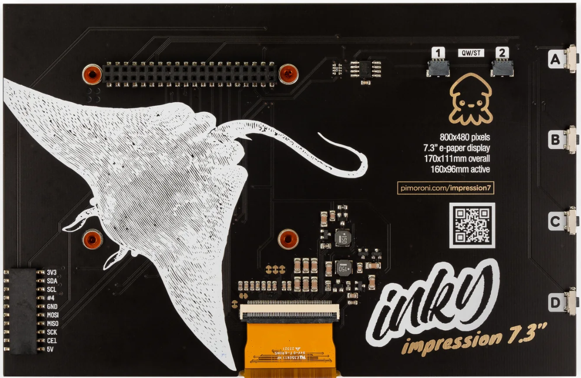
    E-Ink Project - Start

    Let's start from the beginning,

    I'm a tech hoarder with a penchant for collecting embedded development hardware and coming up with projects that force me to learn, often I find myself flipping through projects and leaving things for an extended period when they get hard. After several months, I will face a harder problem as I progress, and looking for respite, I eagerly pick up the original project. Hopefully having a blog will help me launch back in from my drop-off points in the future.

    Such is the case with my e-ink display, several months ago I picked up an 800x480p 7-color e-ink from a local retailer after doing minimal research (Unaffiliated link to the display from Pimoroni); when I went to use it I was surprised to see they only included a Python library! My original use was to have a slow refresh calendar that would update by push from a local server that sent bitmaps to a Raspberry Pi Nano.

    Napkin math makes me reckon that the 800x480 display in a frame buffer would have to represent 512,000 pixels. So with the 264KB of onboard RAM on the Pico I would have to be careful since even a byte per pixel, (512KB), is just under double the total RAM available before even writing any code. Even still, I also presumed that I could use 3 bits for each pixel and have a 154KB data structure for a frame buffer that would also be quicker to iterate through when needed.

    The Python library was a heartbreaker because I would have to use MicroPython. #1, I'm not even sure that's possible, #2, if it is possible I'm still not doing that when there is a wonderful C/C++ SDK for the device. I ended up getting a basic grasp for the few supported use cases of a 45-second refreshing, Python-driven display (with a glass panel, excellent resolution, and color clarity) with Python3 on Pi Zero W.

    Fast Forward to Today

  • Posted on

    The Problem

    For the last two days, I have been reconfiguring my personal network infrastructure to create a complete, secure, and coherent solution for my needs. For context, this server is running systemd Gentoo Linux with +march=native and standard stable compile flags, testing packages are not allowed globally, the kernel is manually configured, it was compiled and installed 12/31. Special care was used to ensure I selected compatible kernel options matching the Gentoo Wiki's article on Docker.

    This issue took longer than I care to admit because of a couple now glaringly obvious red herrings. I was able to emerge and install Docker without a problem, but when I attempted to run the service I received the following error:

    Dec 31 10:34:56 gentoo systemd[1]: Starting Docker Application Container Engine...
    Dec 31 10:34:56 gentoo dockerd[134836]: time="2024-12-31T10:34:56.093036541Z" level=info msg="Starting up"
    Dec 31 10:34:56 gentoo dockerd[134836]: time="2024-12-31T10:34:56.280360174Z" level=info msg="[graphdriver] using prior storage driver: overlay2"
    Dec 31 10:34:56 gentoo dockerd[134836]: time="2024-12-31T10:34:56.280599062Z" level=info msg="Loading containers: start."
    Dec 31 10:34:56 gentoo dockerd[134836]: time="2024-12-31T10:34:56.282787923Z" level=warning msg="Running modprobe bridge br_netfilter failed with message: modprobe: WARNING: Module bridge not f>
    Dec 31 10:34:56 gentoo dockerd[134836]: time="2024-12-31T10:34:56.287999183Z" level=info msg="unable to detect if iptables supports xlock: 'iptables --wait -L -n': `modprobe: FATAL: Module ip_t>
    Dec 31 10:34:56 gentoo dockerd[134836]: time="2024-12-31T10:34:56.340305545Z" level=info msg="stopping event stream following graceful shutdown" error="<nil>" module=libcontainerd namespace=moby
    Dec 31 10:34:56 gentoo dockerd[134836]: failed to start daemon: Error initializing network controller: error obtaining controller instance: failed to register "bridge" driver: failed to create >
    Dec 31 10:34:56 gentoo dockerd[134836]: iptables v1.8.11 (legacy): can't initialize iptables table `nat': Table does not exist (do you need to insmod?)
    Dec 31 10:34:56 gentoo dockerd[134836]: Perhaps iptables or your kernel needs to be upgraded.
    Dec 31 10:34:56 gentoo dockerd[134836]:  (exit status 3)
    Dec 31 10:34:56 gentoo dockerd[134836]: time="2024-12-31T10:34:56.340724371Z" level=info msg="stopping event stream following graceful shutdown" error="context canceled" module=libcontainerd na>
    Dec 31 10:34:56 gentoo systemd[1]: docker.service: Main process exited, code=exited, status=1/FAILURE
    Dec 31 10:34:56 gentoo systemd[1]: docker.service: Failed with result 'exit-code'.
    

    This is where I went naive, the error there clearly indicates iptables is not working properly and the docker service can't properly register it's network configuration causing it to fail. Working through that error log from the bottom up, reviewed all the wiki entries on iptables & ip_tables, I emerged iptables again and once it was finished I attempted to run "iptables -L" which met me with another error shown below. One thing I learned through this is that ip_tables, and iptables, are two related but different things (ip_tables is a kernel module and iptables is a front-end for the module).